O-SiP
Technologies
O-SiP?
LIPAC's O-SiP (Optical-System in Package) is a core component of an optical system by integrating an optical device (Photonic IC) and an electronic device (Electronic IC) into one semiconductor package. There are no restrictions on the types of devices that can be integrated through O-SiP, and they can have different materials (Si, SiGe, InGaAs, InP, Glass) and different functions (analog function, digital function, photonic function). Various devices can be integrated into one semiconductor packaging. Therefore, O-SiP is a versatile 'optical packaging platform' technology that can produce ultra-small, highly integrated optical systems.
"O-SiP: An optical system which can integrate optical devices and electronic devices into one semiconductor packaging"
The O-SiP manufacturing process is based on the advanced semiconductor packaging technology. It is leading the growth of the current semiconductor technology and industry by overcoming the limitation of Moore's law. A prime example of such a change is that the update of the ITRS, which has been the industry standard of Moore's Law, ended in 2015, and the HI Roadmap was newly enacted and became the standard for the semiconductor industry. Therefore, advanced semiconductor packaging technology will continue to advance as one of the main-streams of driving the semiconductor industry and technology in the future.
Among the semiconductor packaging methods, the most advanced technology is Fan Out Wafer Level Package (FOWLP). The conventional semiconductor packaging method uses a way of packaging individual chips one by one, such as the Chip On Board (COB) method or the Flip Chip method as shown in the figure below. This requires wiring and molding for each chip during packaging, so investment in mass production equipment must be made proportional to the increase in quantity.
This packaging method of individual chips has evolved into a method of packaging many chips at once in a wafer level as shown in the figure below. In this case, since wafer processing equipment is used, additional investment costs for production equipment are reduced whereas the quantity increases.
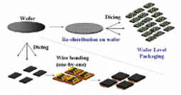
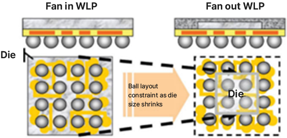
Among the Wafer Level Packaging methods, the WLCSP (Wafer Level Chip Scale Package) method, which packages the wafer without reconfiguration, allows the PAD to be located only within the chip area, so only Fan-In connection is possible as shown in the figure below. In order to overcome this limit to connect a larger number of PADs, fan out wiring is required as shown in the figure below.
In the FOWLP method, the wafer is reconfigured through die rearrangements, and the wiring process is performed using a semiconductor process to connect the fan out connection. In the process of wafer reconfiguration through die rearrangement, multiple dies can be rearranged so that they can be included in the wafer, making it possible to implement System In Package through multiple chips within the package.
O-SiP Structure
The O-SiP can include various structures and functions as shown below.
1. Vertical Optical Direction
| Inside |
Co-packaged IC
|
|---|---|
|
Electrical Connection
|
|
| Outside |
Optical Component
|
|
Electrical Connection
|
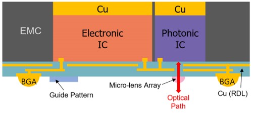
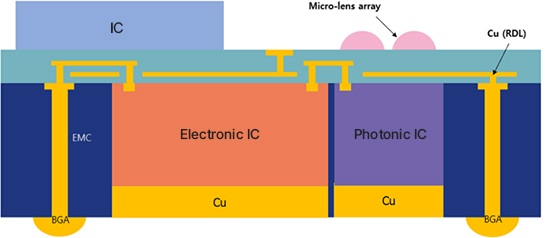
It is an O-SiP structure suitable for optical devices in which light enters and exits perpendicular to the surface of the chip. This is the applicable packaging platform when using VCSEL (Vertical Cavity Surface Emitting Laser), PD (Photodiode), APD (Avalanche Photodiode), LED (Light Emitting Diode). There is no limit to the number of electronic devices that can be included, and various digital and analog devices made of Si, SiGe, GaAs, etc. can also be integrated. Each IC is electrically interconnected within the package by a Redistribution Layer (RDL). Standardized BGA (Ball Grid Array) or LGA (Land Grid Array) can be used for external connection terminals. MLA (Micro Lens Array) and Guide Patterns can be manufactured on the surface, which can be manufactured using a semiconductor process that uses photolithography as a wafer level, enabling precise and efficient manufacturing.
2 . Lateral Optical Direction
| Inside |
Co-packaged IC
|
|---|---|
|
Electrical Connection
|
|
| Outside |
Optical Component
|
|
Electrical Connection
|
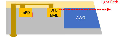
It is an O-SiP structure suitable for optical devices in which light enters and exits horizontally compared to the surface of the chip. Edge emitting laser diodes can be used in this case including DFB (Distributed Feedback) Laser, EML (Electroabsorption Modulated Laser), etc. In addition, monitoring PDs and electronic devices can be packaged together. The O-SiP with vertical and lateral optical direction can be implemented simultaneously within one package.
3. Vertical Optical Direction with stacked IC
| Inside |
Co-packaged IC
|
|---|---|
|
Electrical Connection
|
|
| Outside |
Optical Component
|
|
Optical IC
|
|
|
Electrical IC
|
|
|
Electrical Connection
|
It is a structure that reduces the footprint of packaging by stacking ICs on the package in a two-layer structure. After PAD is formed on the surface of the FOWLP, the stacked chips can be packaged using either Wire Bonding, Flip Chip Bonding, or SMT (Surface Mount Technology) methods.
Advantages of O-SiP
-
1. No limitation on integrated ICs
Since heterogenous integration of various non-custom PICs and EICs is available, producing package products for the wide range of market applications is possible.
-
2. Accurate alignment between ICs
By eliminating optical systems which should be adopted when accurate alignment between ICs is not guaranteed, the form-factor and the cost of a final package product can be minimized.
-
3. High integration of ICs
Because of the compact form-factor of a package, it can be applied to applications where internal space of a module product is highly limited. (ex. Co-packaged optics, mobile phone, wearable devices, etc.)
Since most key components and wiring structure is integrated in a package, it is simple to re-work if there is any failure during assembly process.
-
4. Fine wiring between ICs
By providing fine electrical connections between ICs, signal loss of a high-speed module product can be minimized. (ex. Optical transceiver, co-packaged optics)
Since electrical connections between ICs are provided in a package, no wire-bonding is required during module product assembly process.
-
5. Molding structure encapsulating ICs
Since ICs are encapsulated inside a package, the ICs can be protected from thermal, physical stress and humidity from environment.
-
6. Flexible design availability for heat dissipation structure
Because of flexible package design for heat path from the inside of a package to the outside of a module product, reliability of the module product can be improved.
-
7. Wafer-level production with high yield rate
Since mass production is available using existing infrastructures in the semiconductor industry, over 1 billion units production in a year is possible without additional investment on equipment.
Based on high yield rate which semiconductor process delivers, final cost of a package can be minimized.
O-SiP Manufacturing process
Face Down and RDL Last FOWLP processes are mainly used to produce O-SiP. The standard process sequence is shown below.
-
Chip placement

Using ‘Pick and Place’ machine, components are re-arranged on the adhesive-attached carrier with PAD side down.
-
Wafer level molding

Molding in a wafer level with Epoxy Mold Compound.
-
Release from carrier
Releasing the molded EMC & chips by removing adhesives from carrier, which leads to get re-configured form of wafer.
-
Redisribution layer formation

Forming a Cu re-distribution layer and insulators to connect components after turning over the molded EMC and chips.
-
Lens formation and ball open

Forming the ball grid array for external electrical connections. If necessary, MEMS process is applied to have micro lens array or guide pattern.
-
Singulation

Sawing the wafer in the form of chip package.